Hardware Schematics
Exposed pads
The board was designed with an Open Source philosophy in mind, therefore a few relevant pins are exposed on the pads illustrated below. A user can solder wires to these pads and customize the uThing::VOC board to extend the default functionalities, or prototype new ideas.
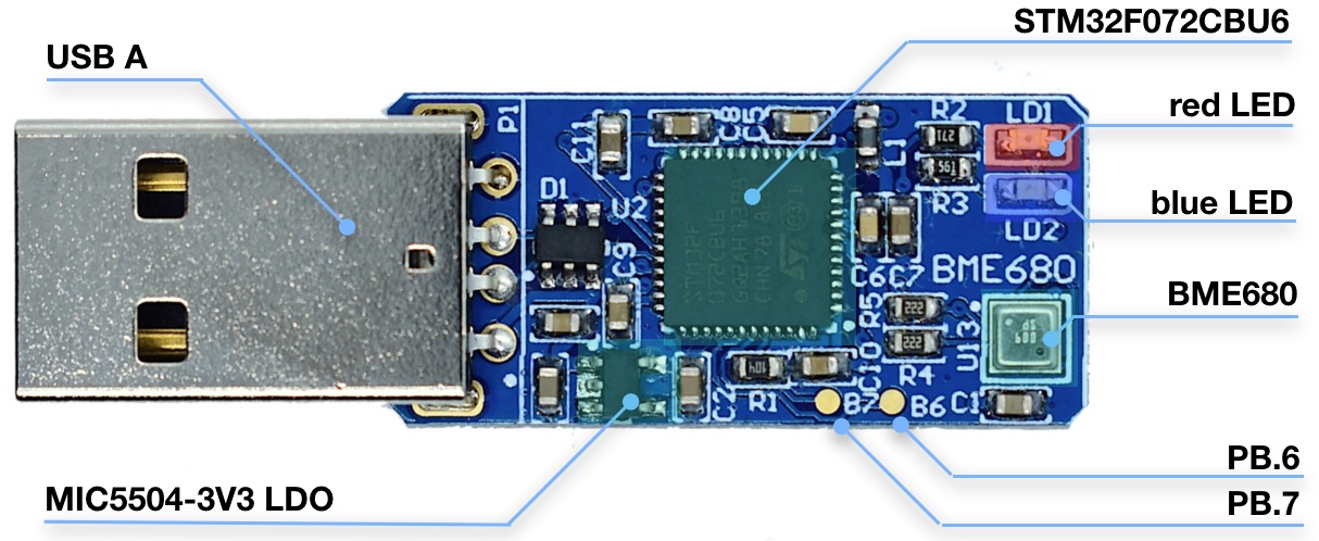
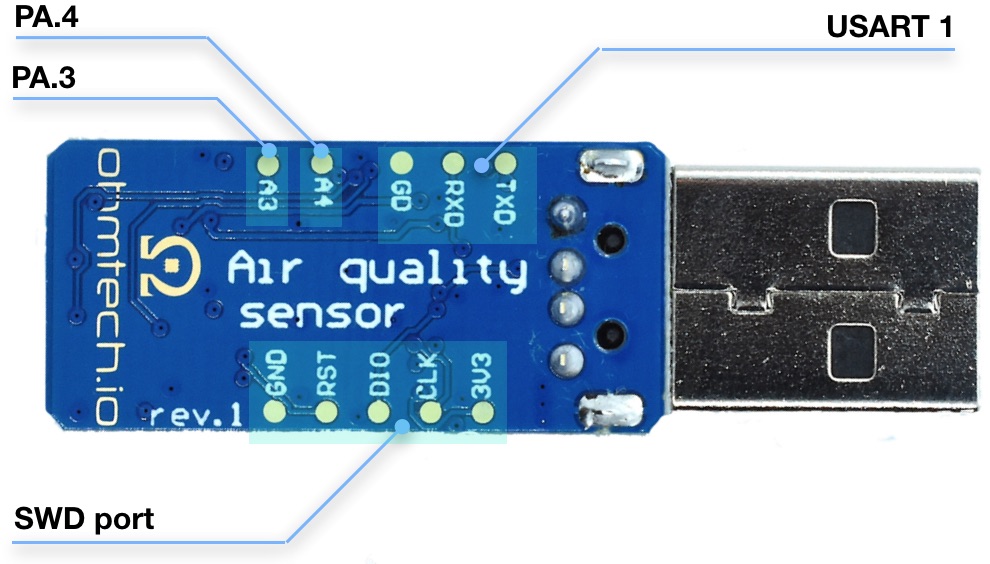
The table below details the connection of the exposed pads and the alternative GPIO functions available:
| ID | Pin # | Signal name | Comment |
|---|---|---|---|
| B6 | 42 | PB.6 | I2C1_SCL (a 2nd I2C bus to avoid any interfering with the BME680) |
| B7 | 43 | PB.7 | I2C1_SDA |
| A3 | 13 | PA.3 | exposes an ADC channel and a timer (PWM out or counter in) |
| A4 | 14 | PA.4 | mapped to an ADC, DAC & Timer channels |
| TXD | 30 | PA.9 | USART1_TXD, TIM1_CH2 (PWM) |
| RXD | 31 | PA.10 | USART1_RXD, TIM1_CH3 (PWM) |
| GD | 8,23,35,47 | GND | System reference ground |
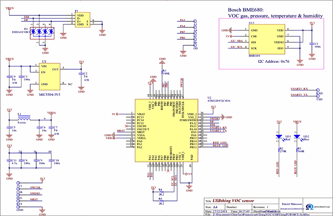
Circuit Schematic
uThing::VOC revision 1 schematic:
(PDF version here)
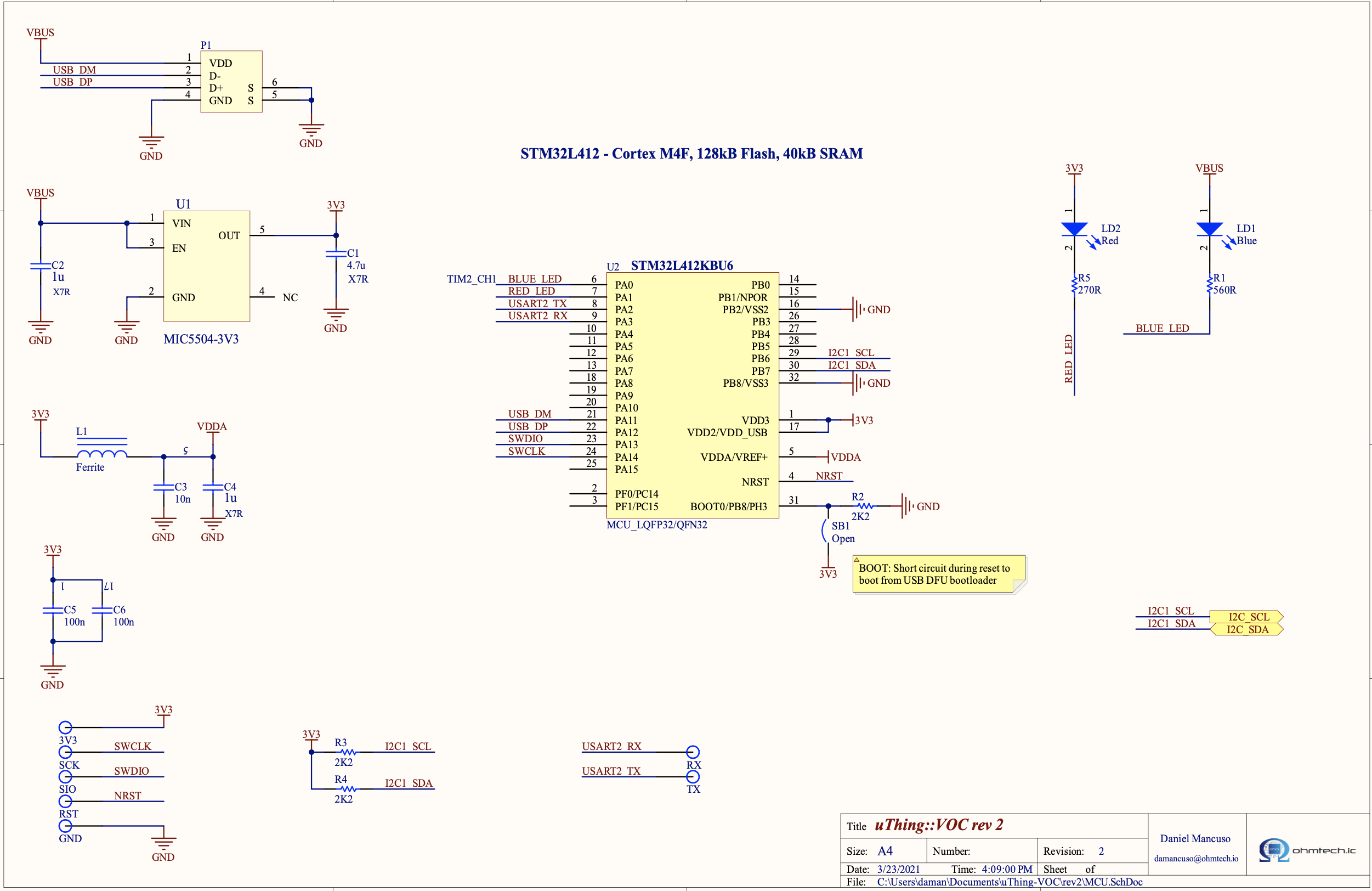
uThing::VOC revision 2 schematic:
(PDF version here)
For more information please check the STM32F072CB datasheet
Design files - source code
The design files (Gerbers, Bill of Materials, Schematics), along with the Firmware source code can be found in the project’s GitHub repositories:
-
Source code repository (MIT License): https://github.com/ohmtech-io/uThingVOC
-
Manufacturing files repository (Creative Commons ShareAlike License): https://github.com/ohmtech-io/uThingVOC-PCB